PCB RF Mean
RF PCBs are the backbone of modern wireless communication systems, radar equipment, satellite technology, and other electronic equipment that uses high-frequency signals. These signals are highly sensitive to various kinds of noise, which is why rf pcb require special design processes and strict guidelines to maintain signal clarity. This article will explore what does pcb rf mean, the most important considerations when designing RF circuit boards, and some of the challenges associated with RF designs.
Unlike other digital signals, RF signals are very susceptible to varying kinds of noise. This includes thermal noise, which occurs when electrons in conductive materials move randomly due to temperature fluctuations. Thermal noise can distort RF signals, leading to reduced sensitivity and accuracy in a receiver’s performance. It can also cause interference, which reduces the quality of an audio or video signal.
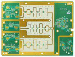
In RF circuits, the characteristics of the conductive materials and the geometry of the components and connections are crucial to maintaining clear signal transmission. This requires that the designer select RF components, like amplifiers, antennas, and filters, with the appropriate frequency range, gain, and noise figure. The designer must also choose a PCB material with the proper dissipation factor and dielectric constant for high frequencies. For example, the common FR-4 substrate has a much higher dissipation factor than more specific high-frequency materials, such as Rogers laminate.
The designer must also ensure that the traces have a characteristic impedance that matches the impedance of the component and connectors. Trace width, shape, and length all affect the characteristic impedance of a PCB. It is essential to follow the PCB manufacturer’s guidelines for trace size and spacing. A trace with the wrong characteristic impedance will cause significant losses and distortion.
What Does PCB RF Mean?
Finally, the designer must pay special attention to minimizing return paths in the circuit design. This can be achieved by placing components close to each other, avoiding routing RF traces near high-speed digital traces or power planes, and using decoupling capacitors between critical components. The designer must also ensure that the RF traces are properly grounded, and provide a solid ground plane beneath the board for optimal operation.
RF circuits are highly sensitive to the characteristics of the PCB material and fabrication process. These can include loss tangent, CTE (coefficient of thermal expansion), and dielectric constant. Choosing the right substrate is crucial, as is the use of plasma etch and laser direct imaging (LDI) equipment for manufacturing. These techniques can ensure that the PCB is manufactured with accurate trace widths and front-to-back registration requirements.
RF circuits are complex and require a specialist supplier to ensure proper production. A trusted PCB manufacturer can work with you to understand the unique needs of your RF circuit, and they can use specialized equipment and materials for high-frequency fabrication. They can also deliver on a quick turnaround and provide a quote within 10 business days.